Shift Register Tutorial for Arduino, ESP8266 and ESP32
Do you know how to increase the number of digital pins for your microcontroller?
With a shift register it is easy to add more digital inputs and outputs to your Arduino, ESP8266 and ESP32 micrcocontroller.
Learn in this article:
- Different configurations of shift register
- What is the right application for each configuration
- In total 3 examples witch different configurations of shift registers and their combination to read the state of multiple buttons to control different LEDs.
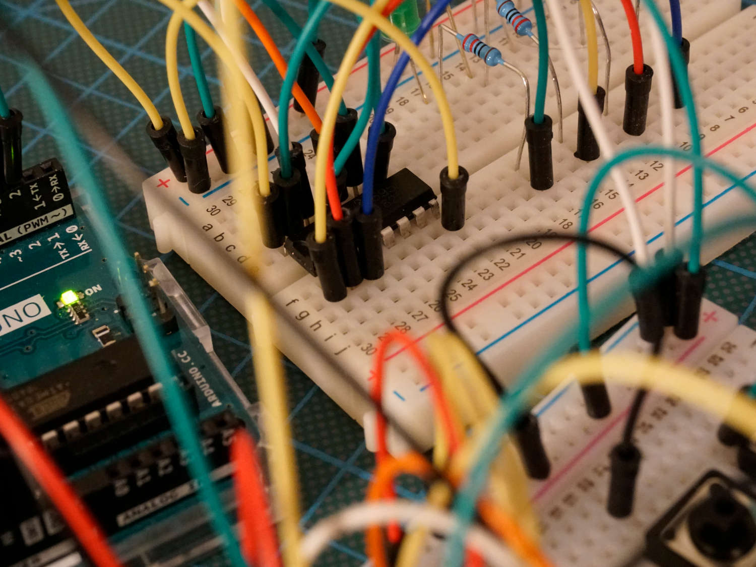
Table of Contents
What is a shift register?
Before I can explain the function of a shift register, you have to know what a flip-flop is, because a shift register is a cascade of multiple flip-flops sharing the same clock signal.
A flip-flop also called latch is a circuit with 2 stable states. These states are often used to store a single bit of information in binary format: 0 or 1.
There are different kinds of flip-flops which is not part of this tutorial. Regarding shift-register we are only interested in the D flip-flop. The D flip-flop has an input line called D, a clock line and an output line Q. The following table shows the truth table of a D flip-flop.
Clock | Data input: D | Data output: Q_next |
Rising edge | 0 | 0 |
Rising edge | 1 | 1 |
Non-rising | 0/1 | Q (output does not change during the clock cycle) |
From the truth table you see that with a rising edge of the clock signal, the output changes to the data line. But if the clock signal is not rising, the output Q_next does not change.
Now basically a shift register is nothing else than multiple D flip-flops connected in a row where the output of each flip flop is connected to the input of the next flip flop. Because there is only one clock signal for all flip flops, a bit is shifted at each clock cycle in the bit array which the bit is stored in.
The following table shows this shifting of a bit if there are three D flip-flops and three clock cycles. At the beginning the bit 1 is in D1 and in each clock cycle this bit is shifted to the next flip-flow until at clock cycle 2 this bit reaches D3.
Clock cycle 0 | Clock cycle 1 | Clock cycle 2 | |
D1 | 1 | 0 | 0 |
D2 | 0 | 1 | 0 |
D3 | 0 | 0 | 1 |
Now we know the basics of the shift register and because shift registers can have parallel and serial inputs and outputs different configurations are possible. Most used configurations are:
- Serial in, serial out (SISO)
- Serial in, parallel out (SIPO)
- Parallel in, serial out (PISO)
From the configurations you can see that shift registers are most used to convert signals between serial and parallel interfaces. In the following sub chapters we take a closer look at each of the configurations.
Serial-In, Serial Out (SISO)
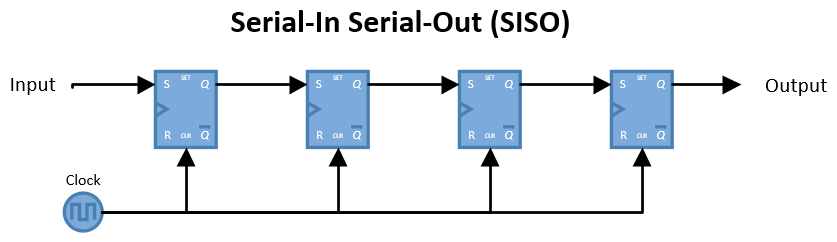
The following table shows the truth table of the SISO shift-register with four flip-flops.
Time | Serial Input | Output |
1 | 1 | 0 |
2 | 1 | 0 |
3 | 0 | 0 |
4 | 0 | 0 |
5 | 0 | 1 |
The SISO shift register configuration is the simplest kind because the input and output are both only one serial line. You might think: What is the use of such a shift register?
If you look at the logic circuit, you see that the SISO consists of n flip flops in a row where is output of the current flip-flop is the input of the next flip-flop. Therefore the input bit is available at the output in n clock cycles. SISO are used to create a time delay in a signal. The most used 8 bit SISO shift register is the 74HC595.
Serial-In, Parallel-Out (SIPO)
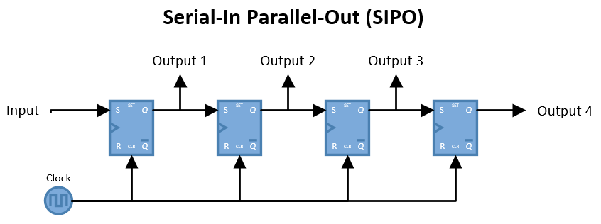
The following table shows the truth table of the SIPO shift-register.
Time | Serial Input | Output 1 | Output 2 | Output 3 | Output 4 |
1 | 1 | 0 | 0 | 0 | 0 |
2 | 1 | 1 | 0 | 0 | 0 |
3 | 0 | 1 | 1 | 0 | 0 |
4 | 0 | 0 | 1 | 1 | 0 |
5 | 0 | 0 | 0 | 1 | 1 |
The serial-input, parallel-output shift register is based on the SISO but after each flip flop there is an output line. This makes the output parallel. The main use of a SIPO shift register is to convert serial data into parallel data, also called demultiplexing. This is very useful when you want to output some data from your microcontroller but there are not enough pins available.
Later in the example we connected the output pin of an Arduino Uno to the serial input of the shift register. The parallel output of the shift register is then connected to multiple LEDs.
The only downside using a SIPO instead of multiple pins on your Arduino or ESP8266 microcontroller is that the connection is slower than the parallel output.
The most used 8-bit SIPO shift registers are 74LS164 and 74LS594.
Parallel-In Serial-Out (PISO)
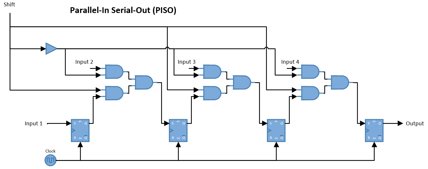
The following table shows the truth table of the PISO shift-register.
Shift Flop 1 | Shift Flop 2 | Shift Flop 3 | Shift Flop 4 | Output |
1 | 0 | 0 | 1 | |
1 | 1 | 0 | 0 | 1 |
1 | 1 | 1 | 0 | 01 |
1 | 1 | 1 | 1 | 001 |
1 | 1 | 1 | 1 | 1001 |
The parallel-in, serial-out has the opposite function then the serial-in, parallel-out shift register. The input is the most significant bit in the array of bits.
If the write/shift line is LOW you can write data into the shift register. The data is shifted from one flip-flop to the next one when the write/shift line is HIGH and at the same time the flip-flops are clocked. In each clock cycle the next bit is shifted to the output and if you have n flip-flops, then the output reads the last bit in n clock cycles.
In the example later in this tutorial we use the PISO to read multiple states of buttons and send this information multiplexed to one digital pin of our microcontroller. The parallel-in, serial-out shift register therefore has the objective to connect multiple inputs if the microprocessor has less I/O pins then needed.
The PISO has the same downside like the SIPO, that the connection is slower than the parallel input.
The most used 8-bit PISO shift register is the 74HC166.
Universal Shift Registers
There are also universal shift registers with a bidirectional usage. That mean, that these registers are able to work in all possible configurations: SISO, SIPO, PISO, PIPO. Unlikely there are no 8-bit universal registers available only 4-bit. If you wan to buy these kind of shift registers you can look aver TTL 74LS194, 74LS195 or CMOS 4035.
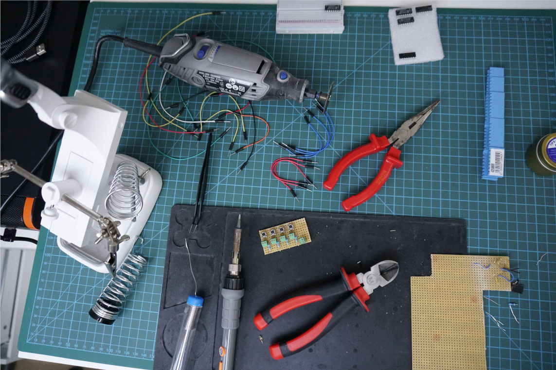
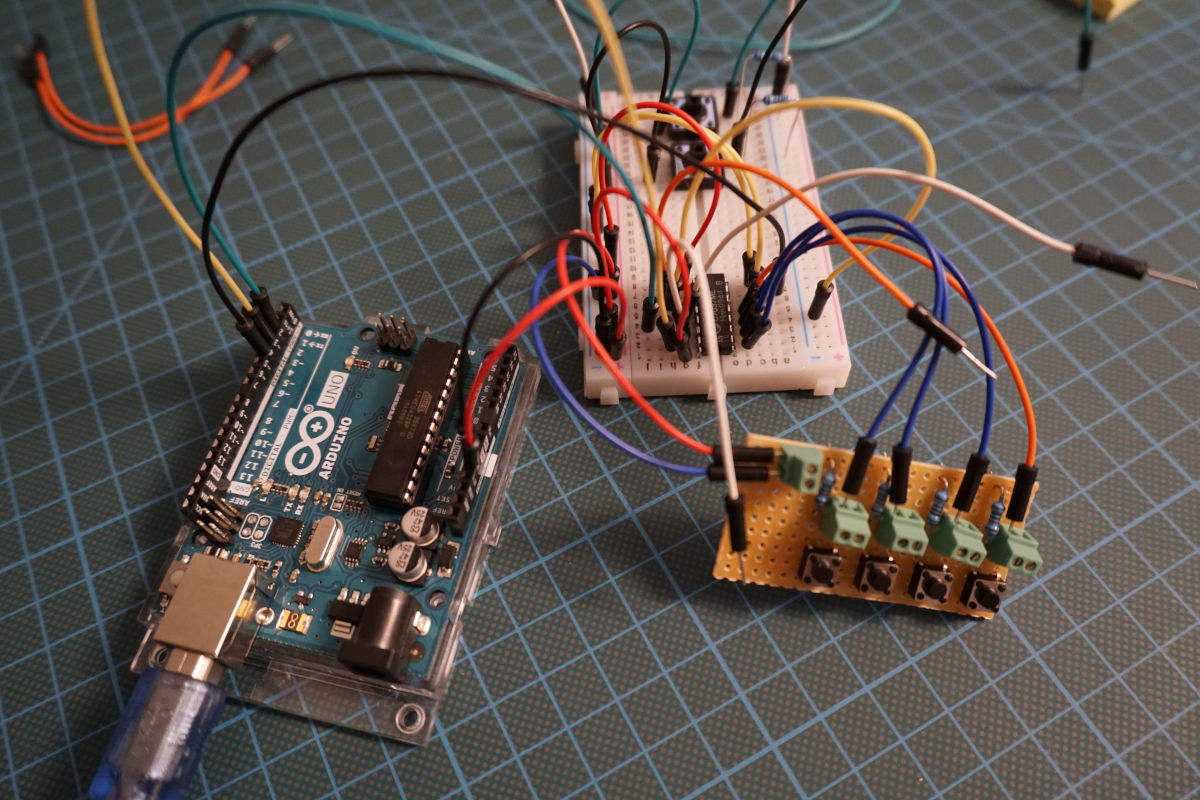
Shift register examples with multiple buttons and LEDs
In the following part of the whole tutorial I want to show you how to use two different shift registers to control multiple LEDs via the state of push buttons. In the first two examples we build up the sketch and program for each shift register individually and in the last example we combine the two examples:
- Create the circuit to control the LEDs with a SIPO shift register 74hc595n. You can obviously use any other SIPO for this example.
- Read the states of multiple push buttons with the 74HC166 PISO shift register.
- Put everything together and control the LEDs with the current states of the push buttons.
Control LEDs with SIPO 74hc595n
The 74hc595n is a Serial to Serial/Parallel 8-bit shift register has an operating voltage between 2V-6V and is therefore best suited for the Arduino or ESP8266 microcontroller. You find the whole data sheet here.
The functionality of the 74hc595n SIPO is easy explained in three steps:
- The latch (STCP pin) is pulled LOW, because the data is only stored in the register on a LOW → HIGH transition.
- Data is shifted out to the register with the data pin (DS) and with a LOW → HIGH transition of the clock signal (SHCP).
- The latch (STCP pin) is released HIGH to save the data in the register.
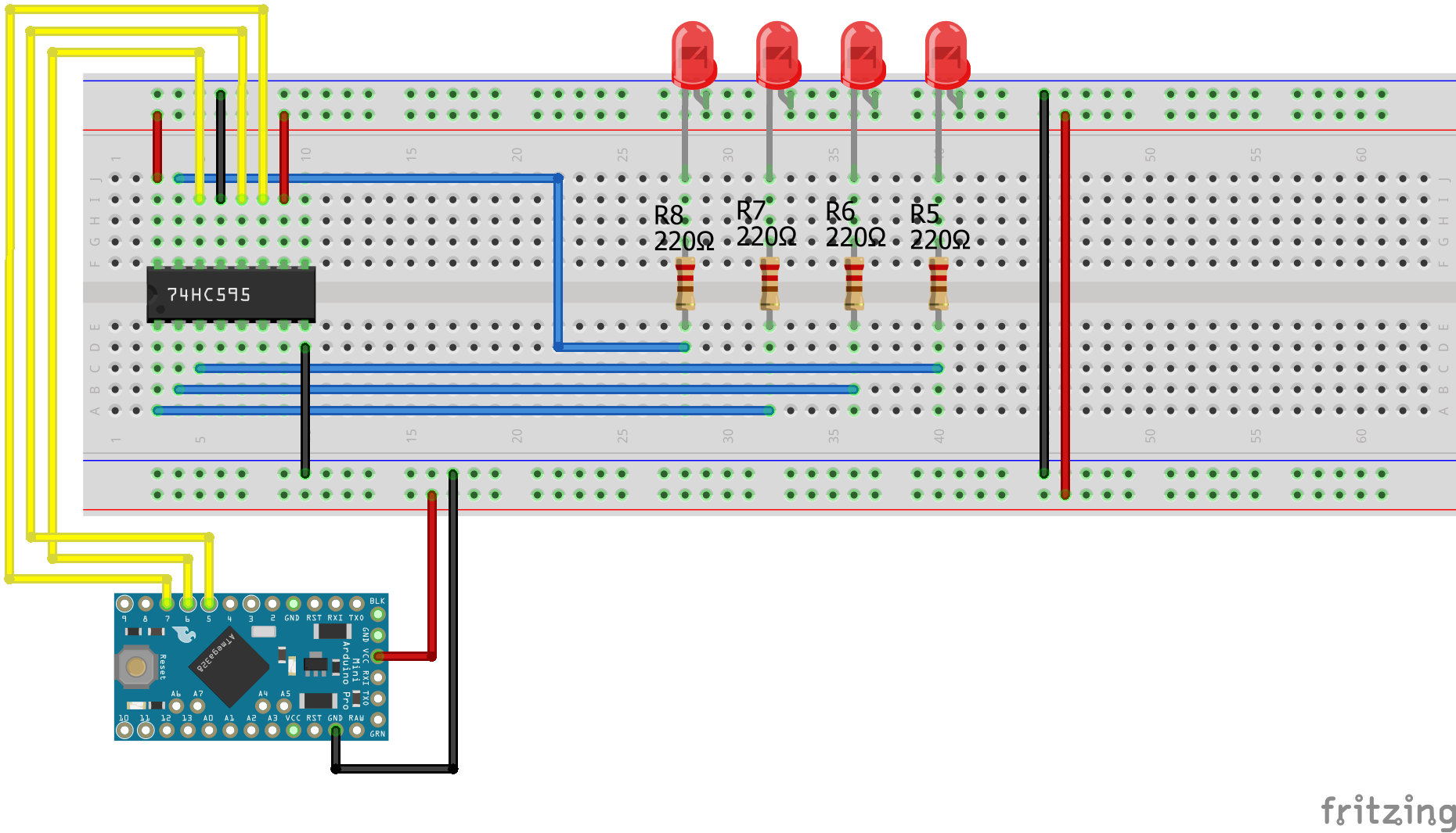
The following pictures show the wiring between the most used Arduino, ESP8266 and ESP32 microcontroller and the 74hc595n as well as the LEDs and resistors.
You can click on each picture to enlarge it. If you are missing your microcontroller, please write me a message in the comment section and I will add your microcontroller to the wiring.
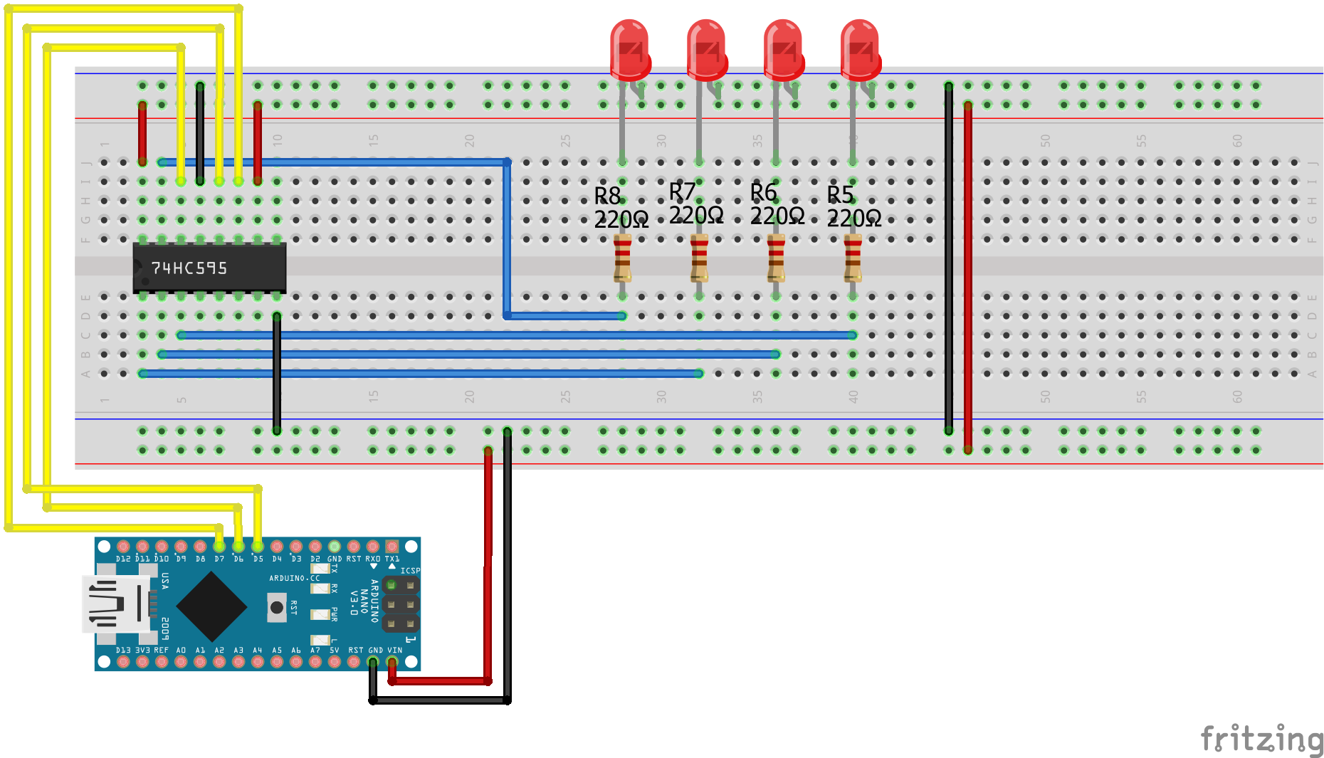
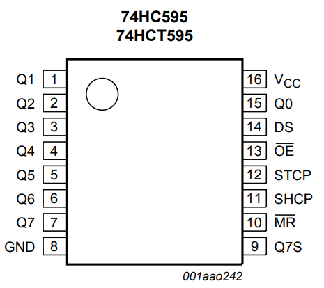
Shift Register SIPO Arduino Nano
Shift Register SIPO Arduino Pro Mini
Shift Register SIPO Arduino Uno
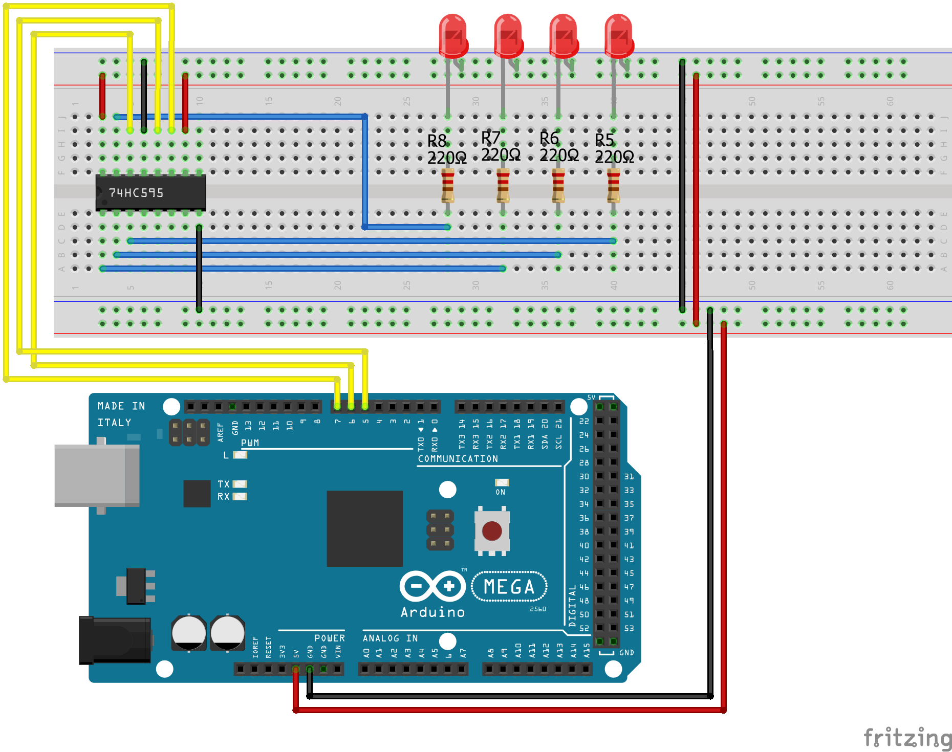
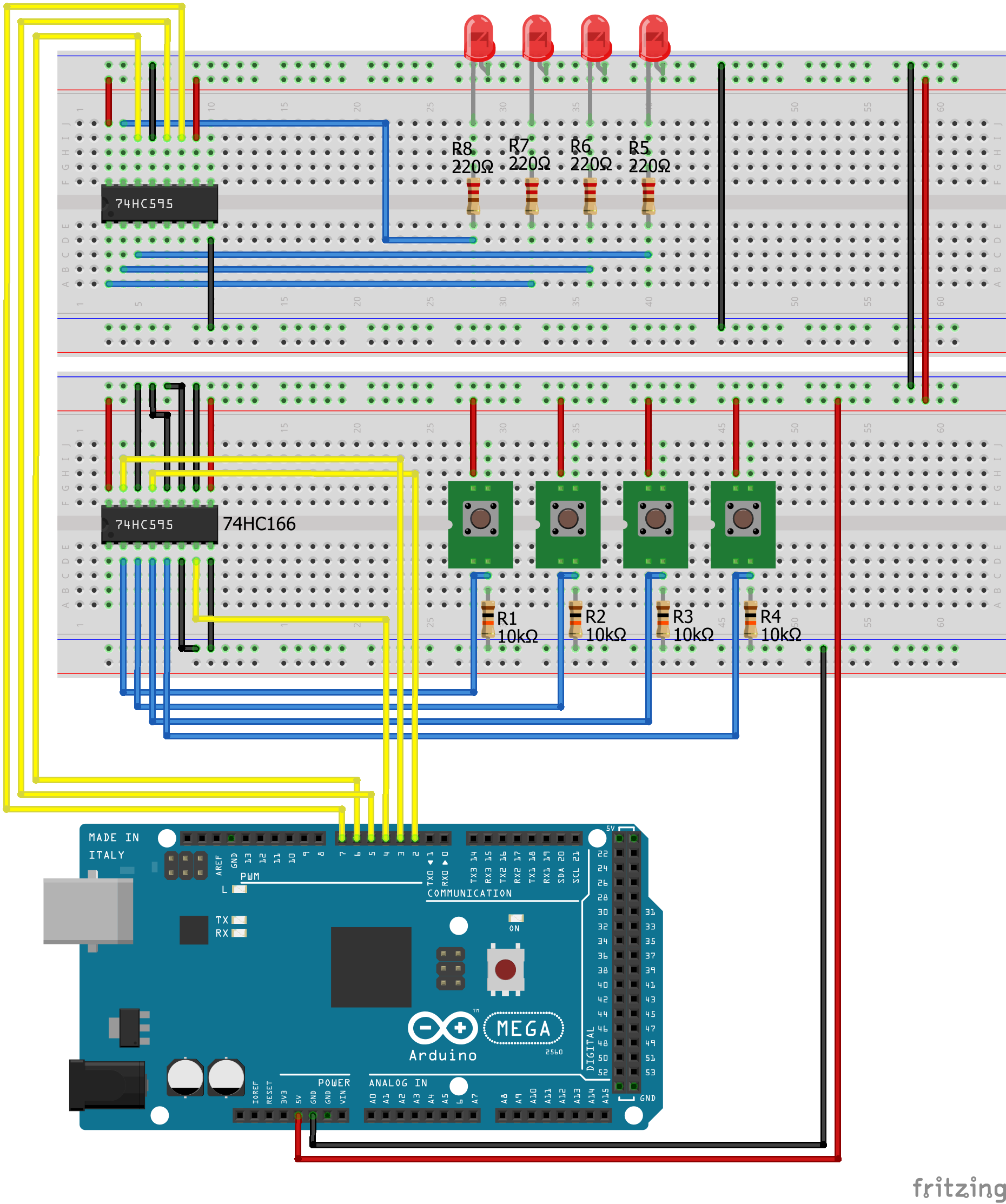
Shift Register SIPO Arduino Mega
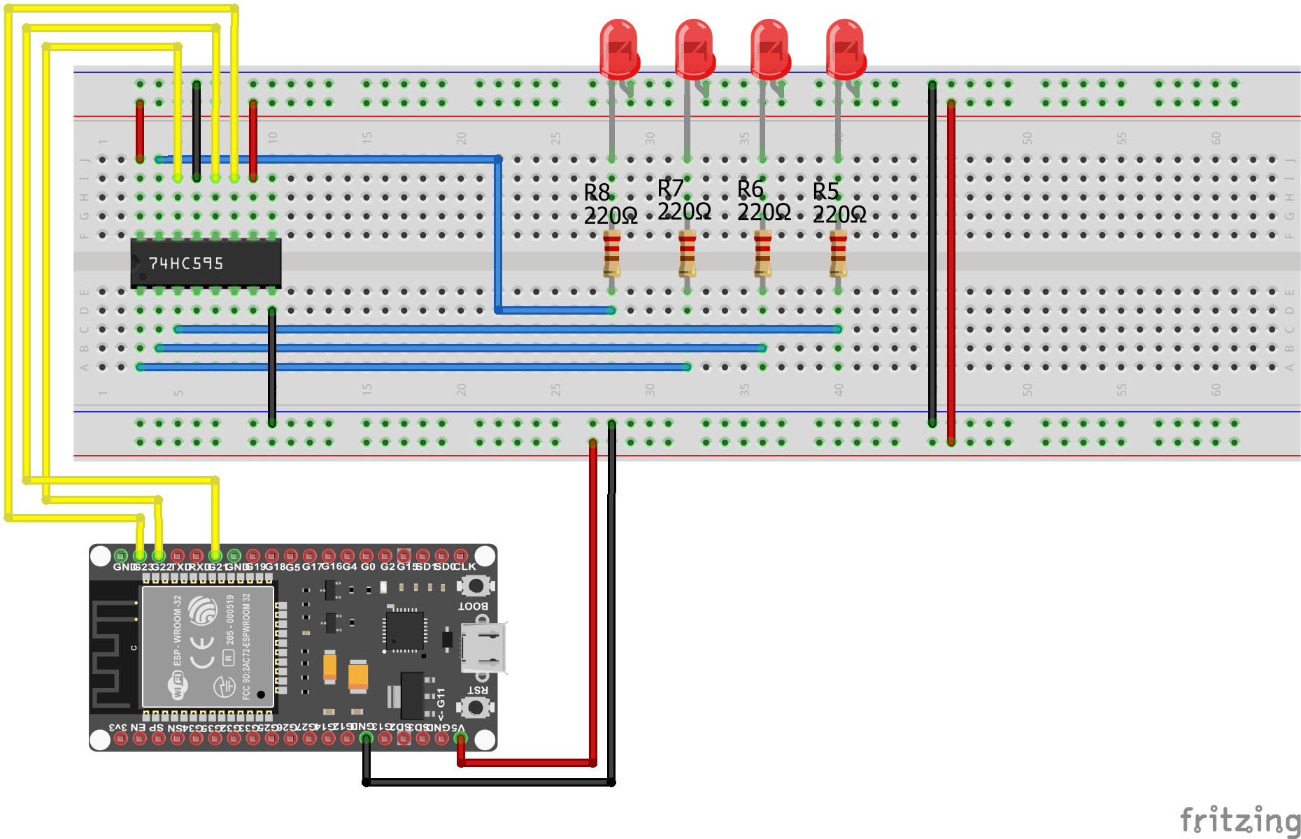
Shift Register SIPO EPS32 NodeMCU

Shift Register SIPO ESP8266 NodeMCU
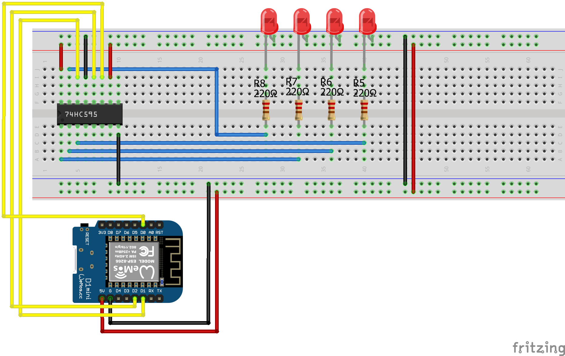
Shift Register SIPO ESP8266 WeMos D1 Mini
The program code is maybe simpler than you think because there is a build in function for the Arduino IDE which shifts data automatically to the shift register. Let us take a look at the code and I explain the lines to you.
// for Arduino Microcontrollers
int latchPin_SIPO = 5;
int clockPin_SIPO = 7;
int dataPin_SIPO = 6;

// for ESP8266 Microcontrollers
//int latchPin_SIPO = D2;
//int clockPin_SIPO = D0;
//int dataPin_SIPO = D1;

// for ESP32 Microcontrollers
//int latchPin_SIPO = 21;
//int clockPin_SIPO = 23;
//int dataPin_SIPO = 22;

byte leds = 0;

void setup()
{
  pinMode(latchPin, OUTPUT);
  pinMode(dataPin, OUTPUT);
  pinMode(clockPin, OUTPUT);

  Serial.begin(9600);
}

void loop()
{
  leds = 0;
  updateShiftRegister();
  delay(1000);
  for (int i = 0; i < 8; i++)
  {
    bitSet(leds, i);
    updateShiftRegister();

    for (int i = 7; i >= 0; i--)
    {
        bool b = bitRead(leds, i);
        Serial.print(b);
    }

    delay(1000);
    Serial.println(" ");
  }
}

void updateShiftRegister()
{
   digitalWrite(latchPin, LOW);
   shiftOut(dataPin, clockPin, LSBFIRST, leds);
   digitalWrite(latchPin, HIGH);
}
First we define the pins for the connection to the 74hc595n. The defined pins depend on the microcontroller. Therefore I added the program code not only for the Arduino pins but also for the ESP8266 and ESP32, but I comment the program lines. You simply have to uncomment the lines for the microcontroller, you have and comment the definition for the other microcontroller.
For all Arduino boards, pin D5 is connected to the storage register clock input (STCP), pin D7 to the shift register clock input (SHCP) and D6 is connected to the serial data input (DS).
If you use an ESP8266 board I use the digital pins D0, D1 and D2 for the storage register and shift register clock input as well was the serial data input.
For the ESP32 NodeMCU I use pin 21, 22 and 23 but you can use different digital pins if you like.
Also we define the variable leds as byte type to later store the information what bit we set to 1 to activate the corresponding LED.
In the setup function we have to declare the pins to the shift-register as outputs and also set the baud rate to 9600.
In the loop function we set the leds variable to zero because we want to initialize the 8-bit array with zeros. Therefore no LED will light up after updating the shift register with the function updateShiftRegister() which I describe in the next section of the code explanation.
After a delay of one second we enter a loop from 0 to 7 and in each iteration we set the next bit in the 8-bit array to 1. After each iteration we update the shift register again with the same function.
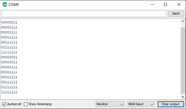
To visualize the array I use another for loop to print every bit in a line. Scroll down to the video to see the screenshot of the serial monitor.
The function updateShiftRegister() takes care that the shift register is updated after each iteration and at the beginning of the for loop. The function executes the same 3 step logic we defined earlier in this article:
- The latch (STCP pin) is pulled LOW, because the data is only stored in the register on a LOW → HIGH transition.
- Data is shifted out to the register with the data pin (DS) and with a LOW → HIGH transition of the clock signal (SHCP). We use the shiftOut function with the last significant bit first.
- The latch (STCP pin) is released HIGH to save the data in the register.
In this example code I use the option of LSBFIRST. Therefore you see in the following video, that the LEDs light up at the end of the for loop as bit 4 to bit 7, starting by the LED connected to Q3.
If I would change the option to MSBFIRST, the LEDs will light up at the beginning starting by the LED connected to Q0. You find the video under the next table.
Bit 7 | Bit 6 | Bit 5 | Bit 4 | Bit 3 | Bit 2 | Bit 1 | Bit 0 | |
LSBFIRST | Q0 (green LED) | Q1 (yellow LED) | Q2 (red LED) | Q3 (blue LED) | Q4 | Q5 | Q6 | Q7 |
MSBFIRST | Q7 | Q6 | Q5 | Q4 | Q3 (blue LED) | Q2 (red LED) | Q1 (yellow LED) | Q0 (green LED) |
The following picture shows the serial monitor as output of the SIPO example.
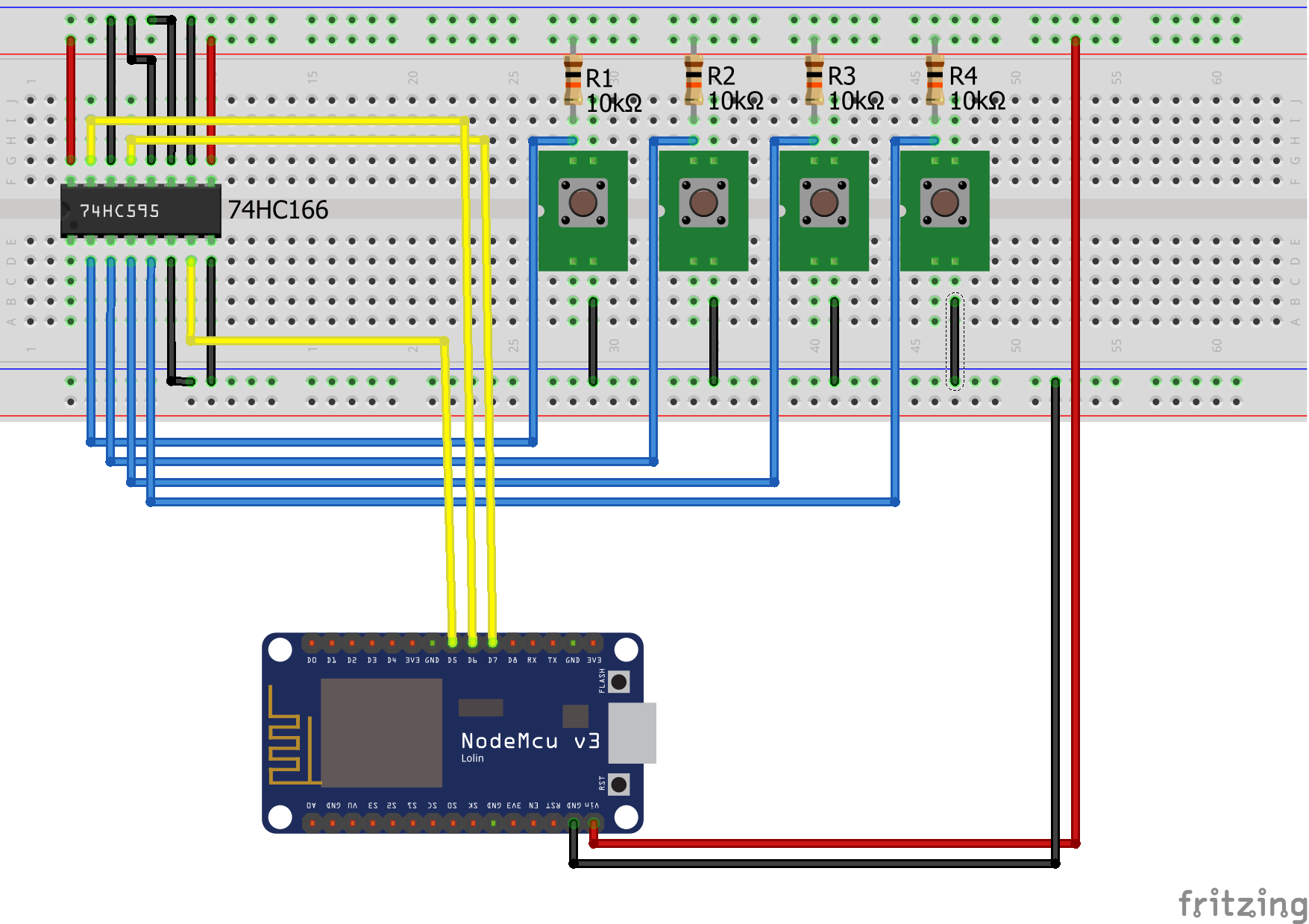
Read the states of multiple buttons with the 74HC166 PISO
The 74HC166 is an 8-bit serial or parallel-in / serial-out shift register. For the power supply, the minimal voltage is 2V, the maximum voltage is 6V with a typical voltage of 5V. Therefore the 74HC166 can be used with an Arduino as well as with a ESP8266 microcontroller.
If you are interested in the whole datasheet, you find it on this website.
The right picture shows the pins of the 74HC166 which I describe in the following section.
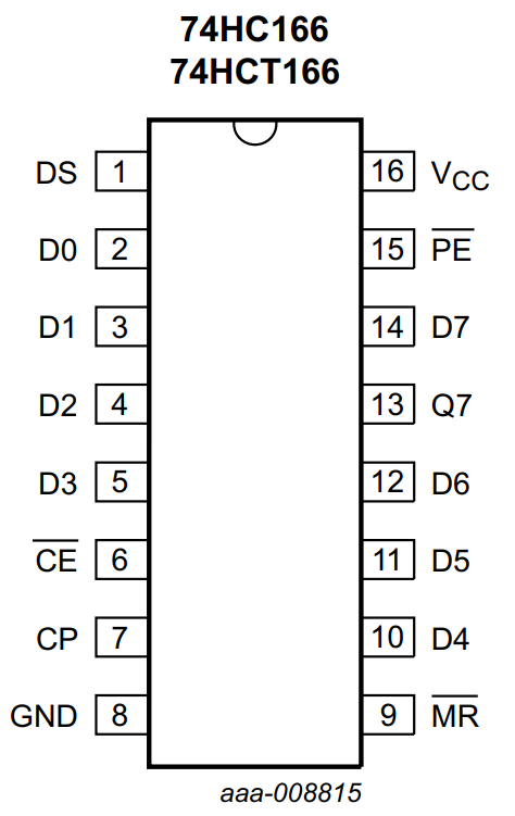
74HC166 pin | Description and Connection |
D0...D7 | Parallel inputs of the shift register to read up to 8 signals with only 3 pins on your Arduino or ESP8266 microcontroller |
GND | Connect to ground on the microcontroller |
VCC | Connect to 5V on the microcontroller |
DS | Serial data input not needed and therefore not connected |
CE | Clock enable input is active when low and therefore connected to ground |
CP | Clock input is active on the edge from LOW to HIGH and connected to the microcontroller (in this example D4) |
PE (Latch) | Parallel enable input and connected to the microcontroller (in this example D3) |
MR | Master reset connected to VCC because is active with LOW and we do not want to reset the register |
Q7 | Serial data output from the last stage has to be connected to the microcontroller (in this example D2) |
The following three steps describe the functionality of the 74HC166 shift register:
- First we set the latch (PE pin on D3) and the clock (CP pin on D4) LOW.
- On the LOW to HIGH transition of the clock pin data from D0…D7 is loaded into the shift register.
- Then PE is set HIGH to activate the serial mode of the register to transmit the collected data via the data line to the microcontroller with every LOW to HIGH transition of CP.
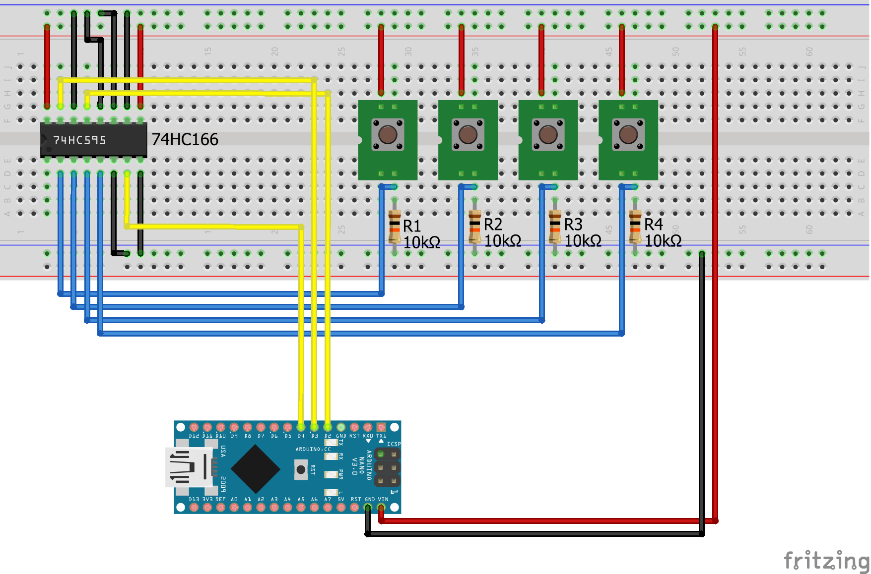
After we know how the 74HC166 is working, the next step is the wiring of the circuit to read the states of the buttons via the 74HC166 shift register.
At this point you have to make a decision which will influence the programming code because you can make a pull-down or a pull-up circuit with the buttons.
- Pull-down configuration: If the button is not pressed the digital signal is LOW = 0
- Pull-up configuration: If the button is not pressed the digital signal is HIGH = 1
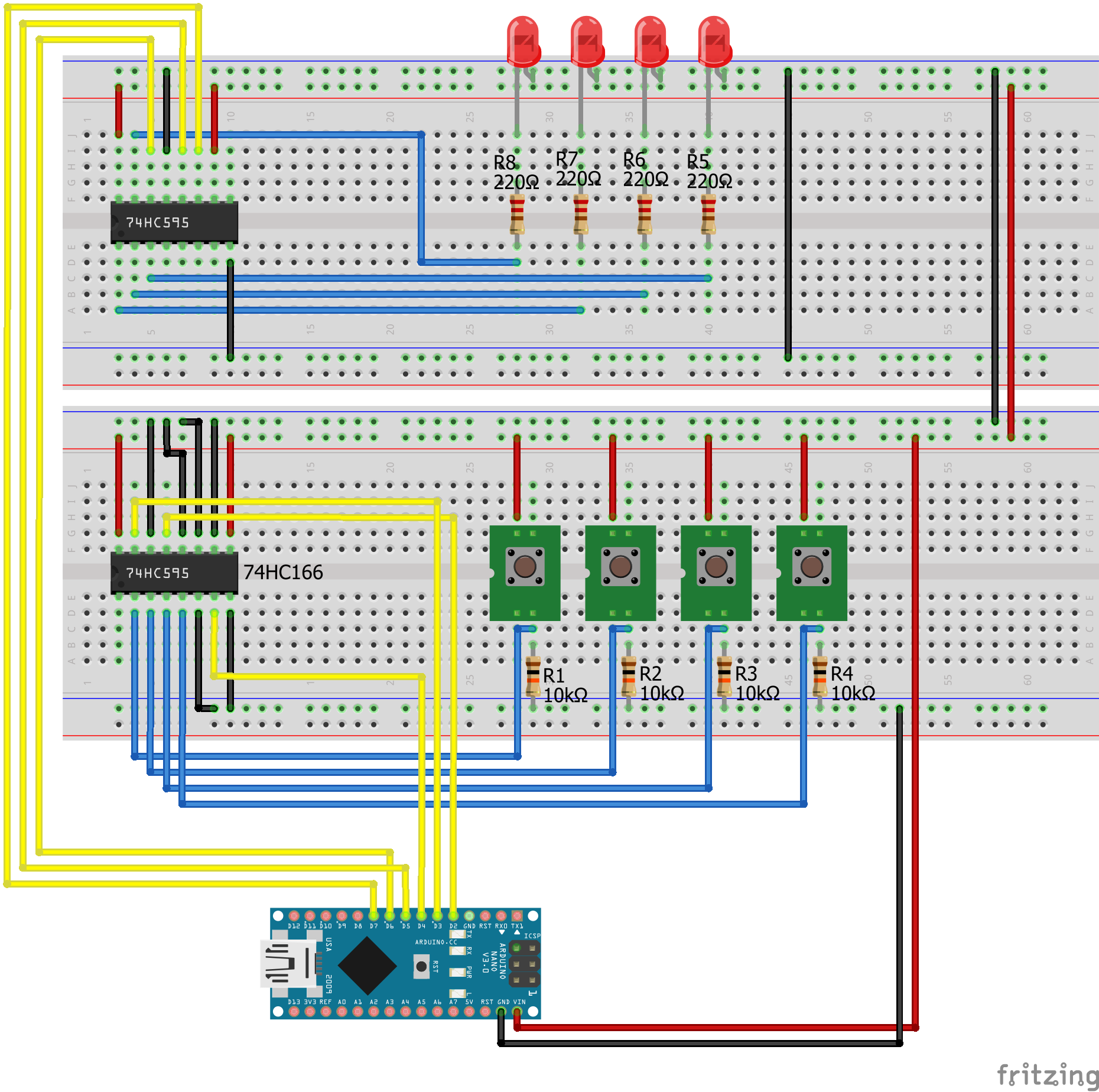
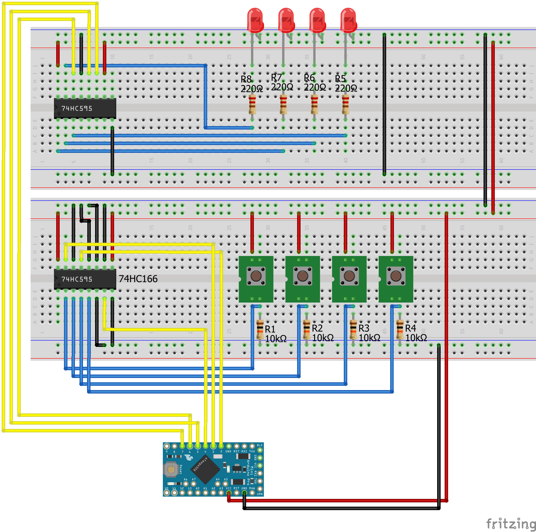
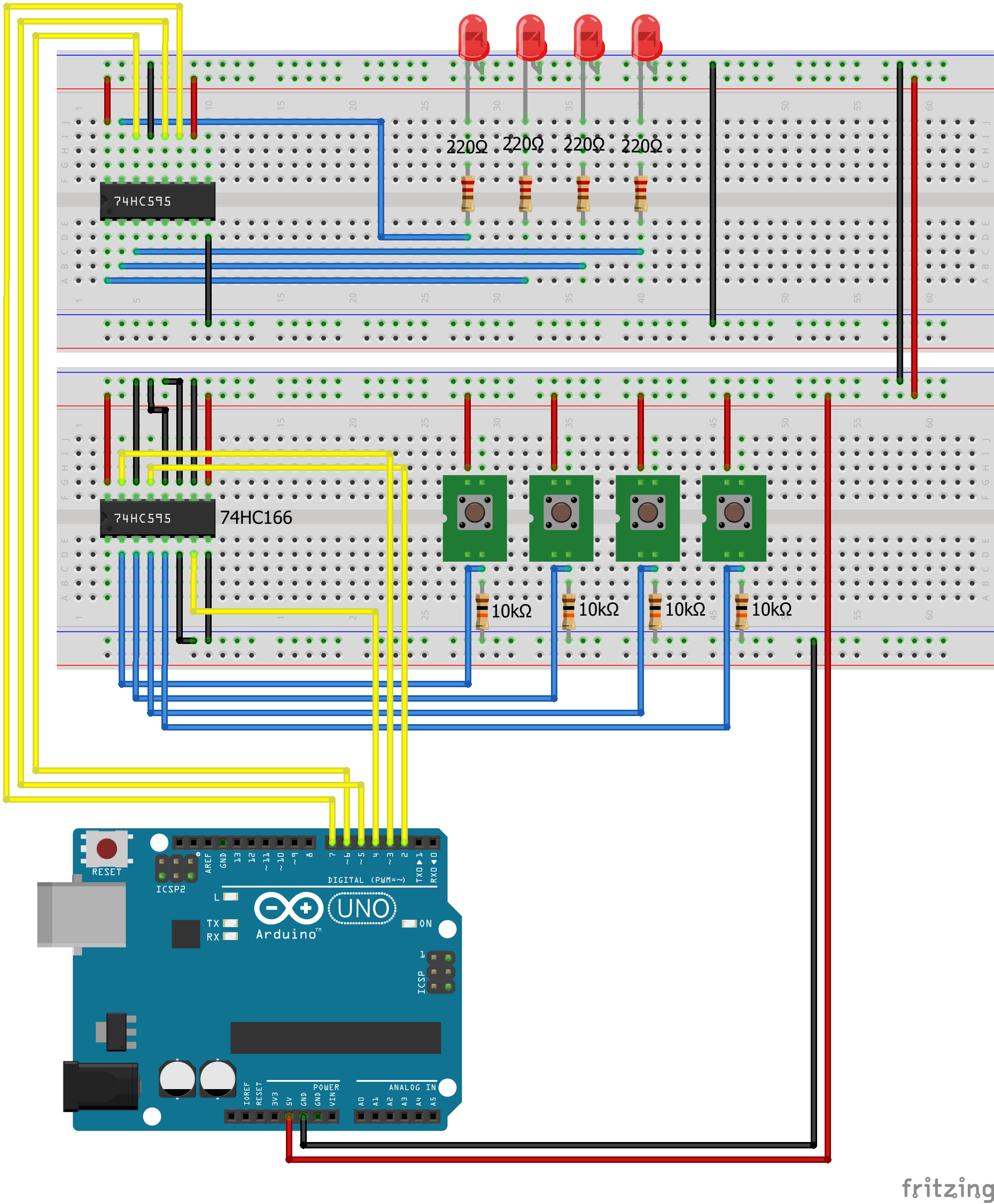
The following two pictures show how I am creating a board for the pull-up configuration to save some wires 🙂
If you are not sure if you know the differences in a pull-down or pull-up configuration, I recommend to read this article where I explain the differences and function in detail.
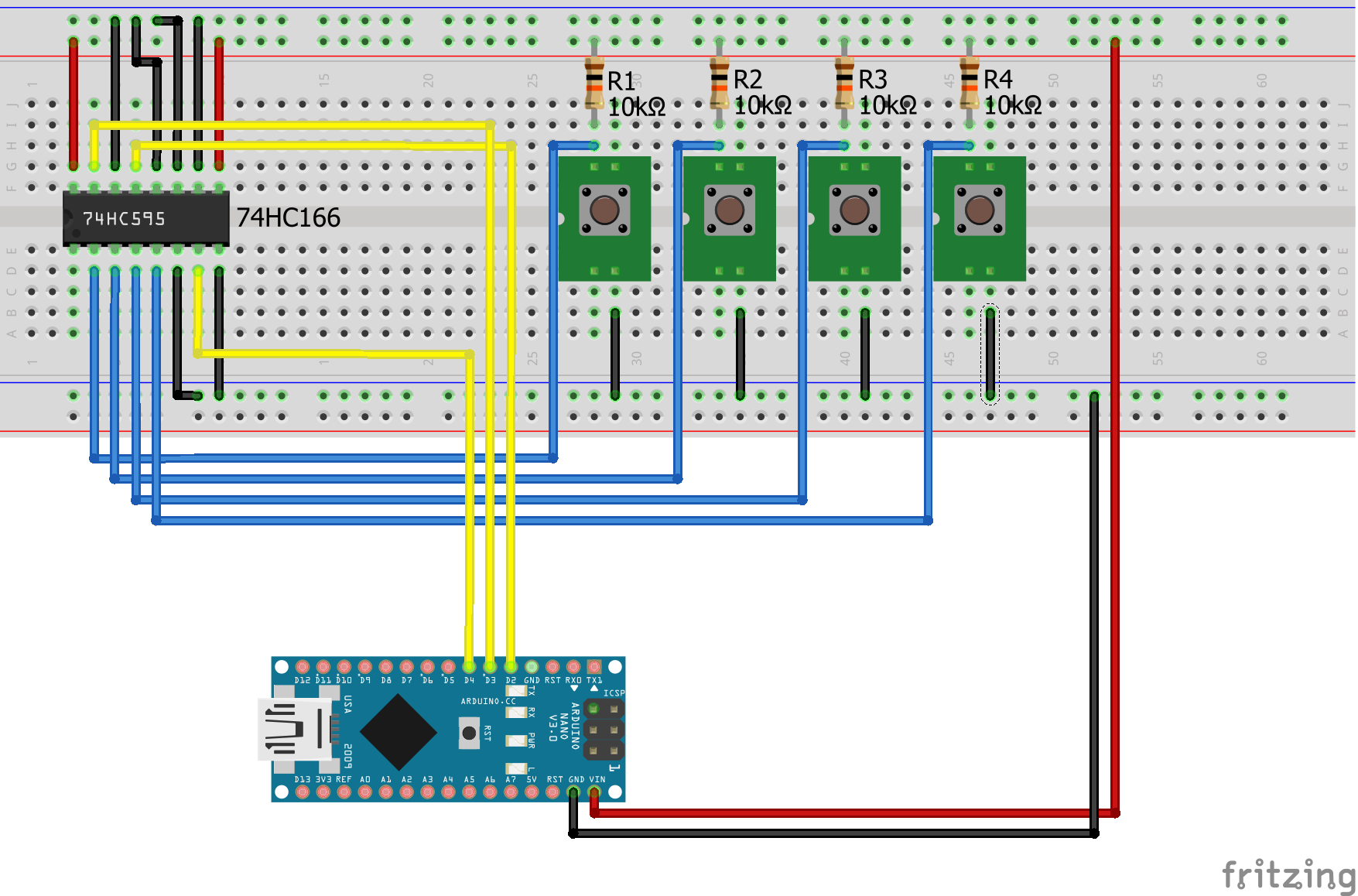
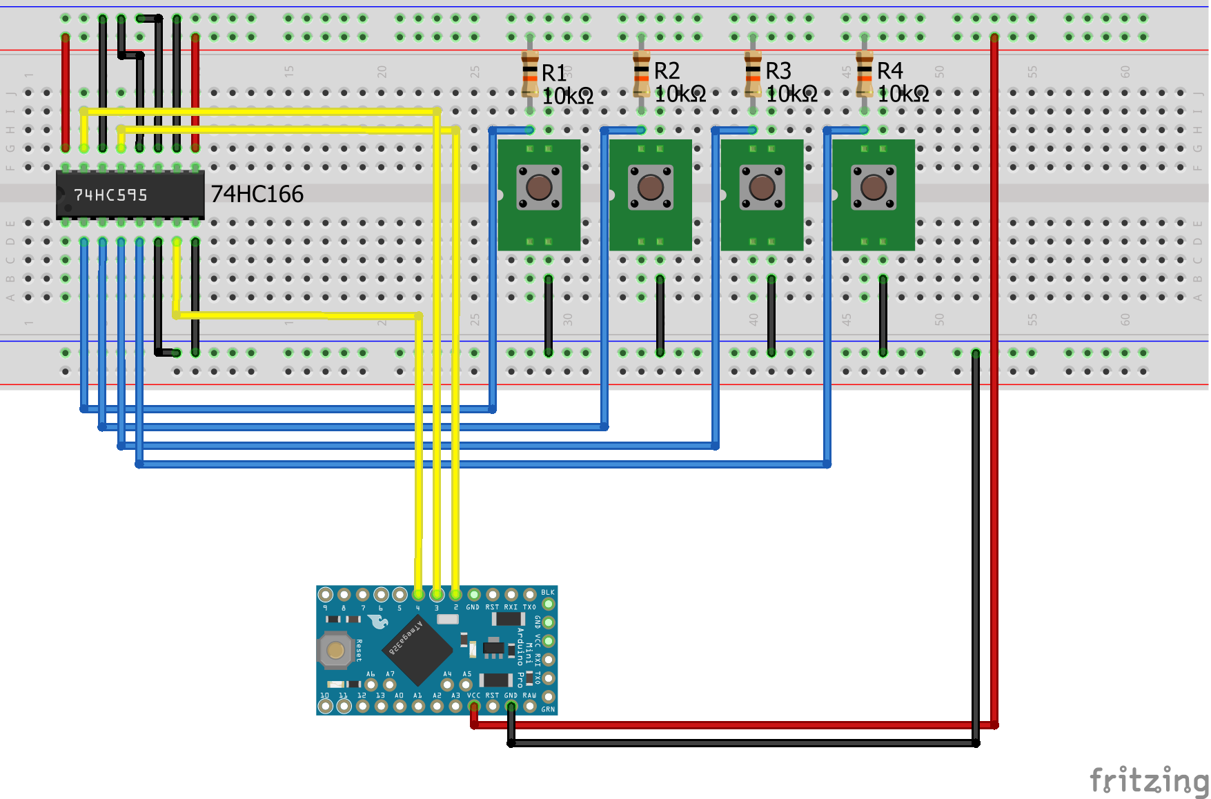
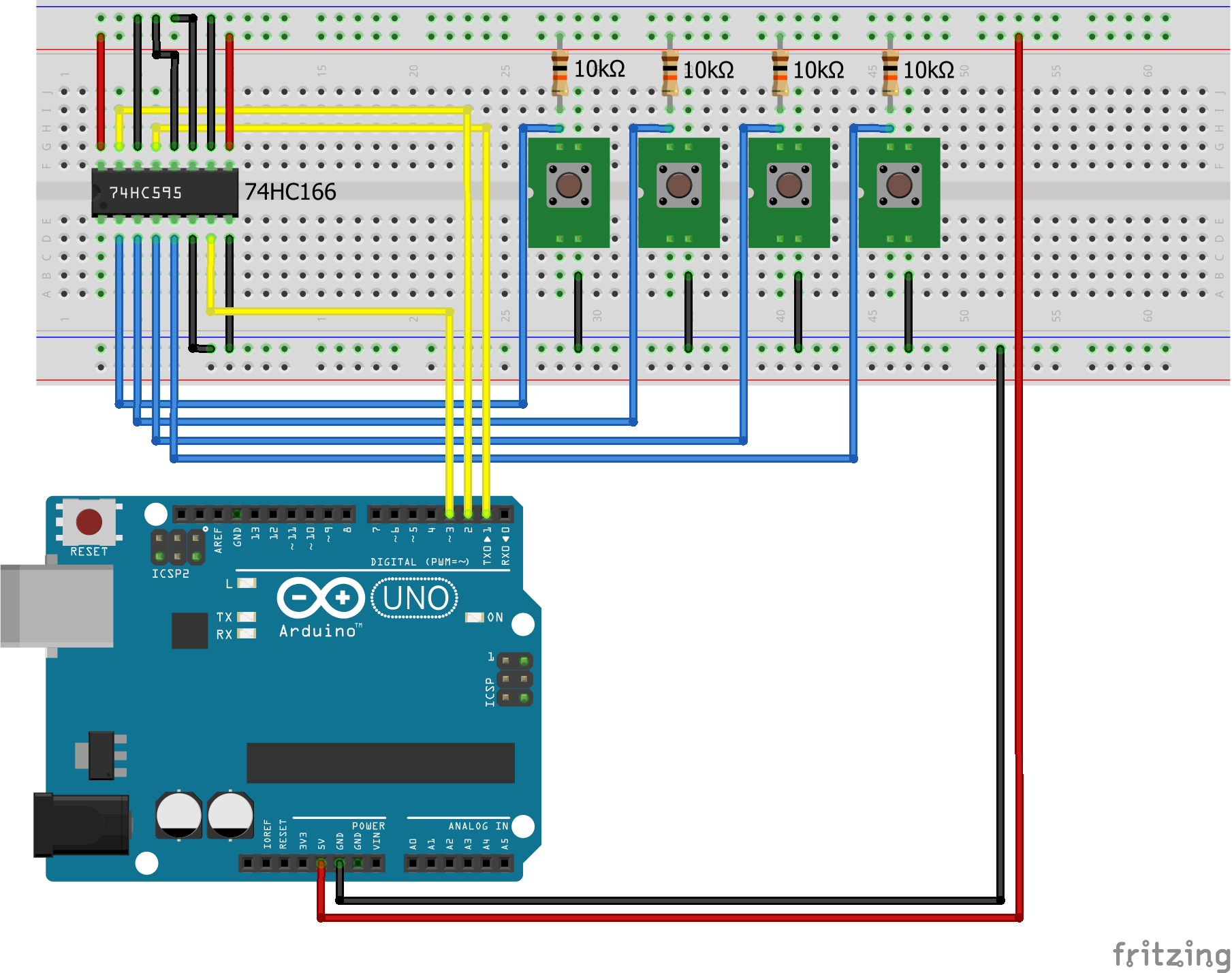
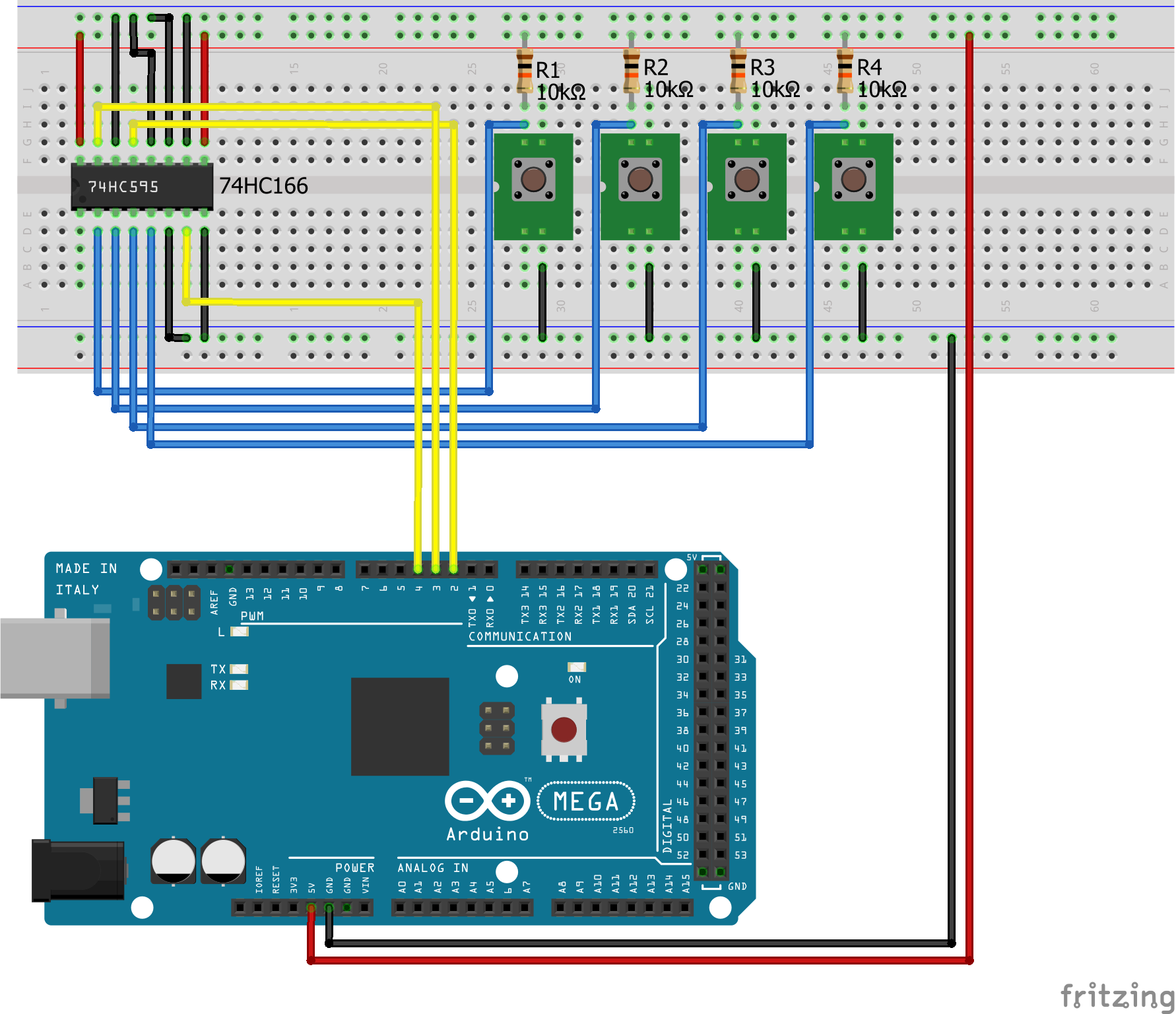
I prepared both configurations for this tutorial to provide you the best possible knowledge. The following pictures shows the fritzing sketch of the PISO shift register in the pull-down and pull-up configuration. Either for both configurations we use 10kΩ resistors.
Shift Register PISO Pull-Down Configuration
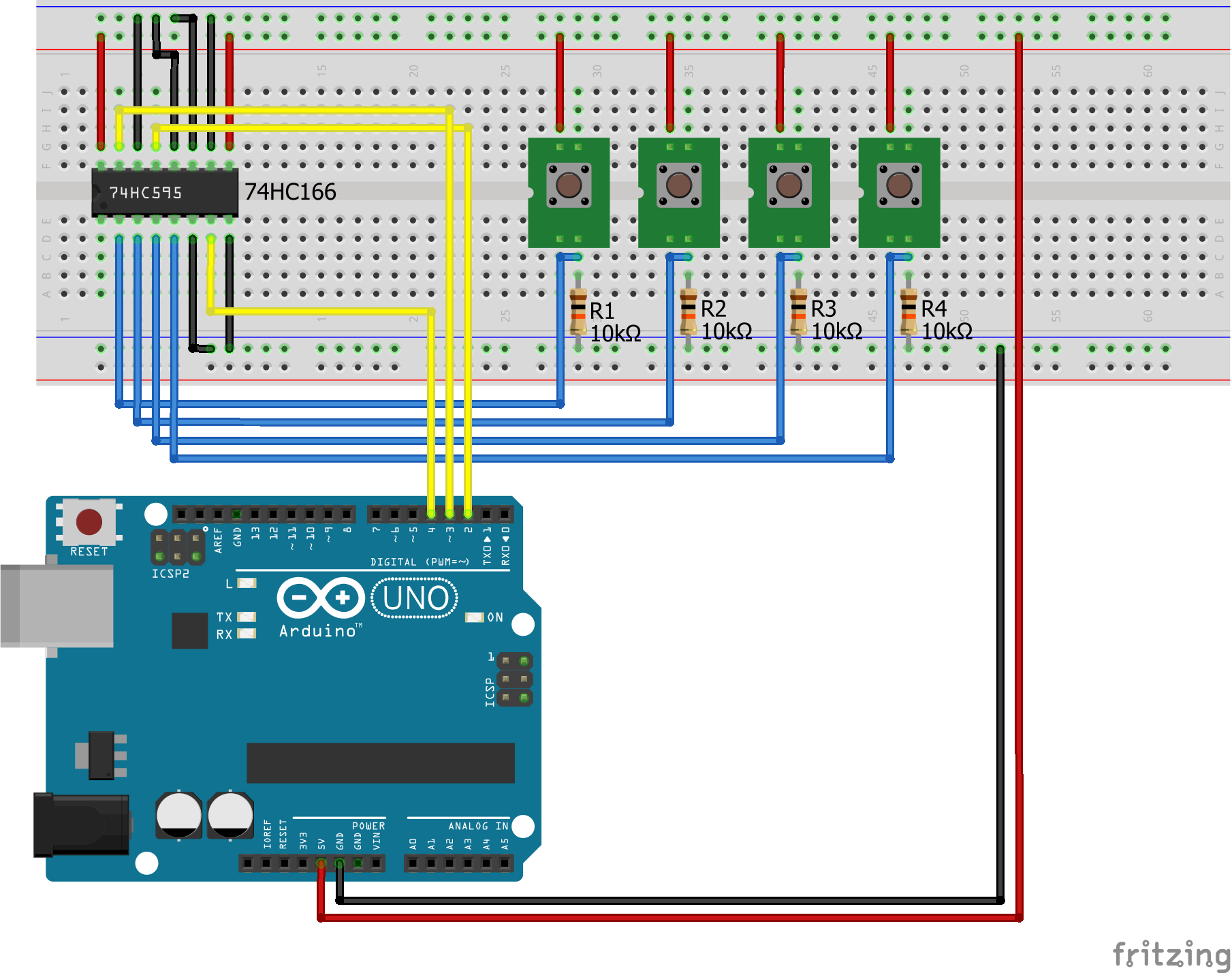
To detect the pushed button you have to set all other values of the 8-bit shift register to 0 if you choose the pull-down configuration because the pushed button will pull the digital line HIGH = 1.
Shift Register PISO Pull Down Arduino Nano

Shift Register PISO Pull Down Arduino Pro Mini
Arduino Shift Register PISO Pull-Down Arduino Uno
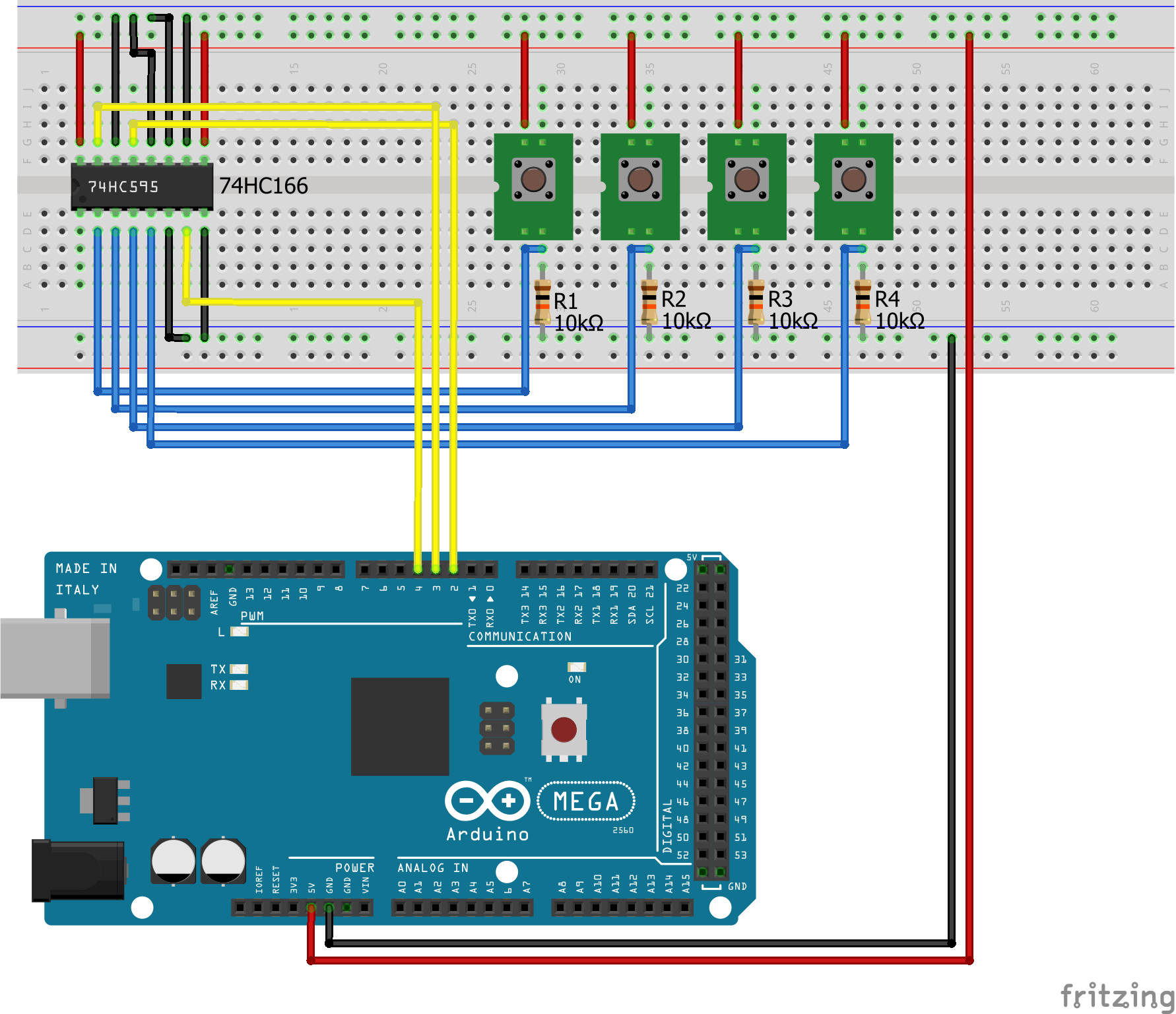
Shift Register PISO Pull Down Arduino Mega

Shift Register PISO Pull Down EPS32 NodeMCU
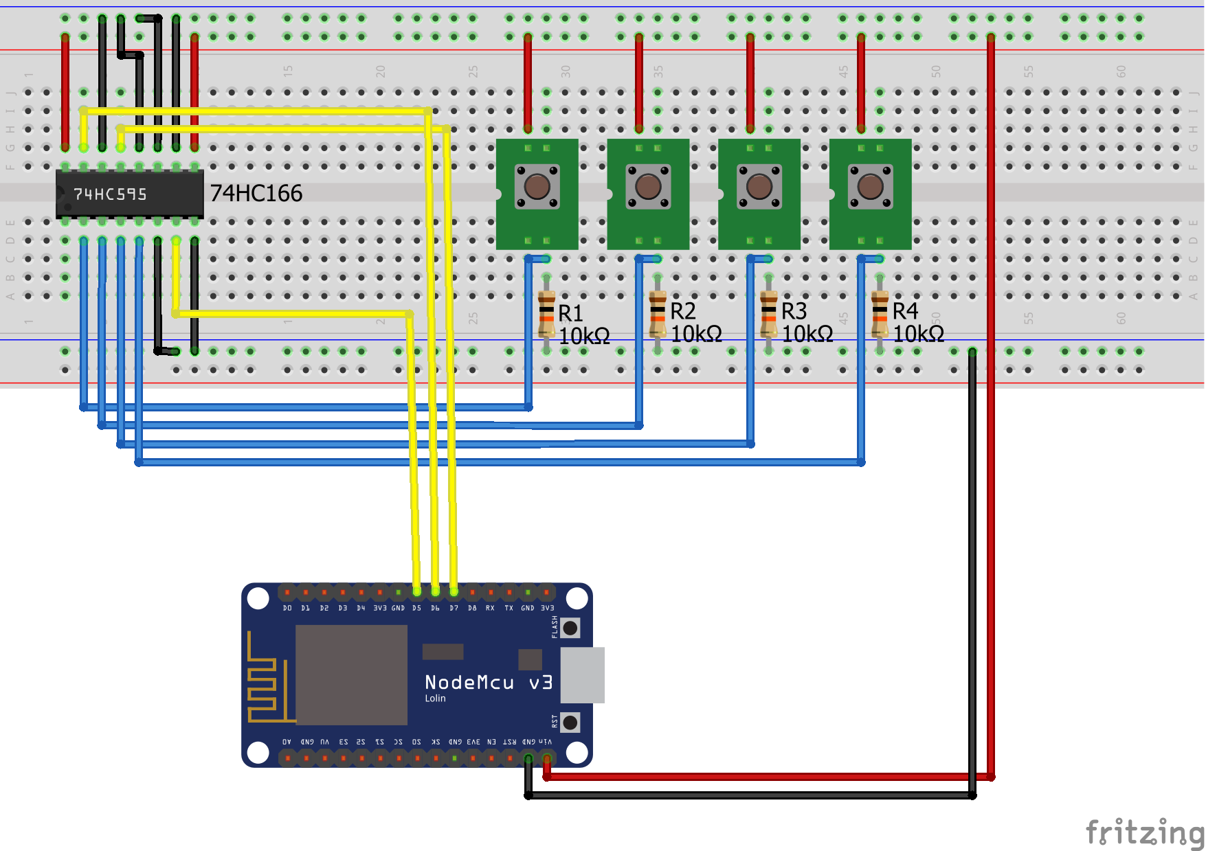
Shift Register PISO Pull Down EPS8266 NodeMCU
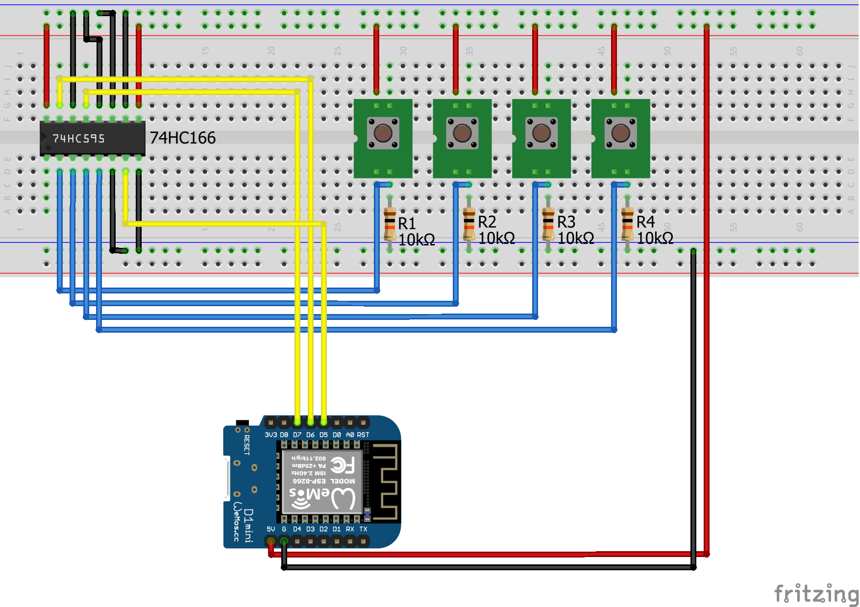
Shift Register PISO Pull Down EPS8266 WeMos D1 Mini
Shift Register PISO Pull-Up Configuration
But if you choose the pull-up configuration you can set all other pins to 1 to detect the pushed button, which sends a 0, when pushed. In my case I do not set all other pins to 1 because I know exactly which bit is changing from 1 to 0 if I press a button. You only have to connect the pins not to ground but to the 5V rail.
Shift Register PISO Pull Up Arduino Nano
Shift Register PISO Pull Up Arduino Pro Mini
Arduino Shift Register PISO Pull-Up Arduino Uno
Shift Register PISO Pull Up Arduino Mega
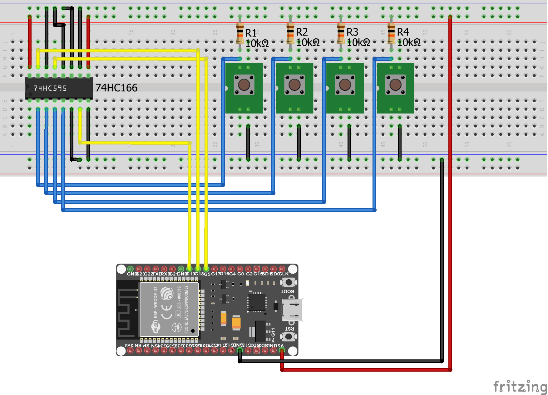
Shift Register PISO Pull Up EPS32 NodeMCU
Shift Register PISO Pull Up EPS8266 NodeMCU

Shift Register PISO Pull Up EPS8266 WeMos D1 Mini
After everything is set up and all components are connected we can go over to the program script. The objective of this example is to display the state of four buttons in the serial monitor.
// for Arduino Microcontrollers
int latchPin_PISO = 3;
int clockPin_PISO = 4;
int dataPin_PISO = 2;

// for ESP8266 Microcontrollers
//int latchPin_PISO = D6;
//int clockPin_PISO = D5;
//int dataPin_PISO = D7;

// for ESP32 Microcontrollers
//int latchPin_PISO = 18;
//int clockPin_PISO = 19;
//int dataPin_PISO = 5;

int j;
int value;
byte switchVar = 0; // for pull down configuration
//byte switchVar = 1; // for pull up configuration

void setup() {
  pinMode(latchPin, OUTPUT);
  pinMode(dataPin, INPUT);
  pinMode(clockPin, OUTPUT);

  Serial.begin(9600);
}

void loop() {
  byte dataIn = 0;
  digitalWrite(latchPin, 0);
  digitalWrite(clockPin, 0);
  digitalWrite(clockPin, 1);

  digitalWrite(latchPin, 1);

  for(j = 0; j < 8; j++) {
    value = digitalRead(dataPin);
    Serial.print("Position of Bit in 8-bit array: ");
    Serial.println(j);
    Serial.print("Value of Bit in 8-bit array: ");
    Serial.println(value);
    if (value) {
      int a = (1 << j);
      dataIn = dataIn | a;
      }
      digitalWrite(clockPin, LOW);
      digitalWrite(clockPin, HIGH);
    }

    if (switchVar != dataIn)
    {
      switchVar = dataIn;
      Serial.print("dataIn DEC: ");
      Serial.print(dataIn, DEC);
      Serial.println();
      Serial.print("dataIn BIN: ");
      Serial.print(dataIn, BIN);
      Serial.println();
    }
  delay(5000);
}
Like in the first example of this tutorial, the first part is to define the pins which connect the microcontroller with the PISO shift register. The latch pin is connected to digital pin 3, the clock to pin 4 and the data line is connected to the digital pin 2.
Also we need three more variables:
- j: used in a for loop to declare which bit is set to 1
- value: stores the digital read value of the data pin
- = 0 if no button is pressed
- = 1 if a button is pressed
- switchVar: stores a byte array to show which button was pressed depending on the pull-down or pull-up configuration
In the setup function, the latch and clock pin are defined as outputs and the data pin as input. Also the baud rate is set to 9600.
In the loop function we start the functionality of the 74HC166 shift register as described before in this article by pulling the clock and latch LOW. Then the clock is pulled HIGH to load the data into the shift register. By also pulling the latch HIGH the previously loaded data is sent to the microcontroller via the serial data line.
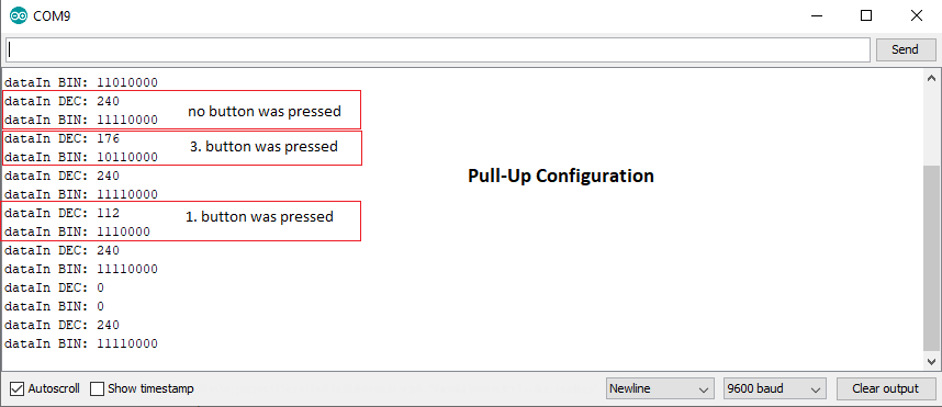
Now we want to find out which button was pressed. Therefore we scan all 8 possible bits in a for loop and read the digital data pin. In the following picture you see the scanning of all 8 bits and you also see that the last two bits are 1 because I pressed two buttons at the same time. Also note that I used the pull-down configuration of the buttons for this picture because only the bits are 1 for which the buttons is pressed and all other bits are 0.
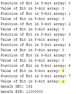
If the value for this bit is 1, there is a bit-shift (<<) of a single bit for the value j. This bit-shifted value is the input of a bitwise OR operation with the variable dataIn. The following table shows this operation in the individual steps:
j | value | a | dataIn |
0 | 0 | 0000 0000 | 0000 0000 |
1 | 0 | 0000 0000 | 0000 0000 |
2 | 0 | 0000 0000 | 0000 0000 |
... | ... | ... | ... |
7 | 1 | 0100 0000 | 0100 0000 |
8 | 1 | 1000 0000 | 1100 0000 |
Also if the data is transmitted from the 74HC166 to the Arduino or ESP8266 microcontroller, the clock line has to be set LOW and HIGH because only in the LOW to HIGH transition, data is transferred.
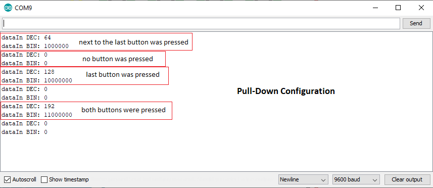
At this point in the script we know that one or more buttons are pressed and we also know which buttons they are. With an if statement we check if there is a change in the variable and if so we print the decimal and binary value of the dataIn variable to the serial terminal.
At the end of the script there is a delay set to 5000 for debugging or to 500 if you want to run the script more frequently.
The following two picture show the difference in the pull-down and the pull-up configuration. In the pull-down configuration all bits are set to 0 and if a button is pressed, the bit is set to 1. For the pull-down configuration all connected bits are set to 1 and only the bit which is pressed is set to 0. For a better detection you could set all bits to 1 by connecting the open bits not to ground but to the 5V rail. Also you have to change the variable switchVar from 0 to 1 to notice the change of the button that is pulled low.
Control multiple LEDs via buttons
Now we put the examples of the SIPO and PISO together in one example. We want to control the LEDs with the buttons. If button 1 is pressed, LED 1 should turn on and so on. I choose the pull-down configuration with only two buttons for this example because all my other buttons which fit on the breadboard are defect but I want to light up a third LED when both buttons are pressed at the same time.
The following picture shows the fritzing sketch of this example where we combine the PSIO and SIPO example. The wiring is shown in the different tabs for the most popular Arduino microcontroller as well as for the ESP8266 and ESP32 microcontrollers.
Click on an image to see the wiring as fullscreen.
Shift Register SIPO PISO PullDown Arduino Nano
Shift Register SIPO PISO PullDown Arduino Pro Mini
Arduino Shift Register SIPO PISO Pull Down
Shift Register SIPO PISO PullDown Arduino Mega
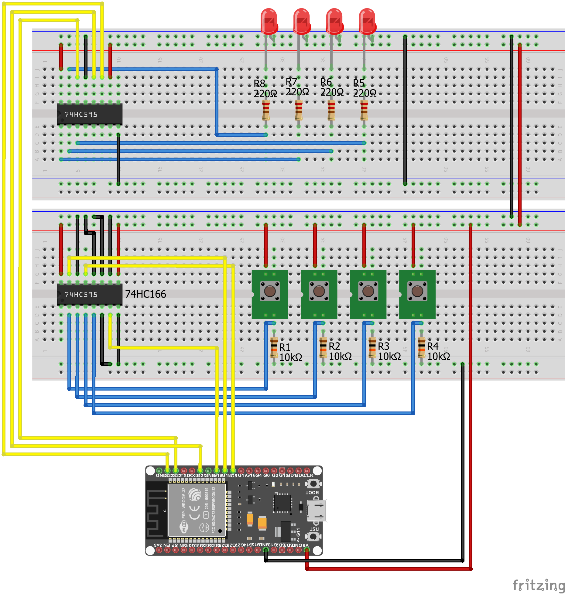
Shift Register SIPO PISO PullDown EPS32 NodeMCU
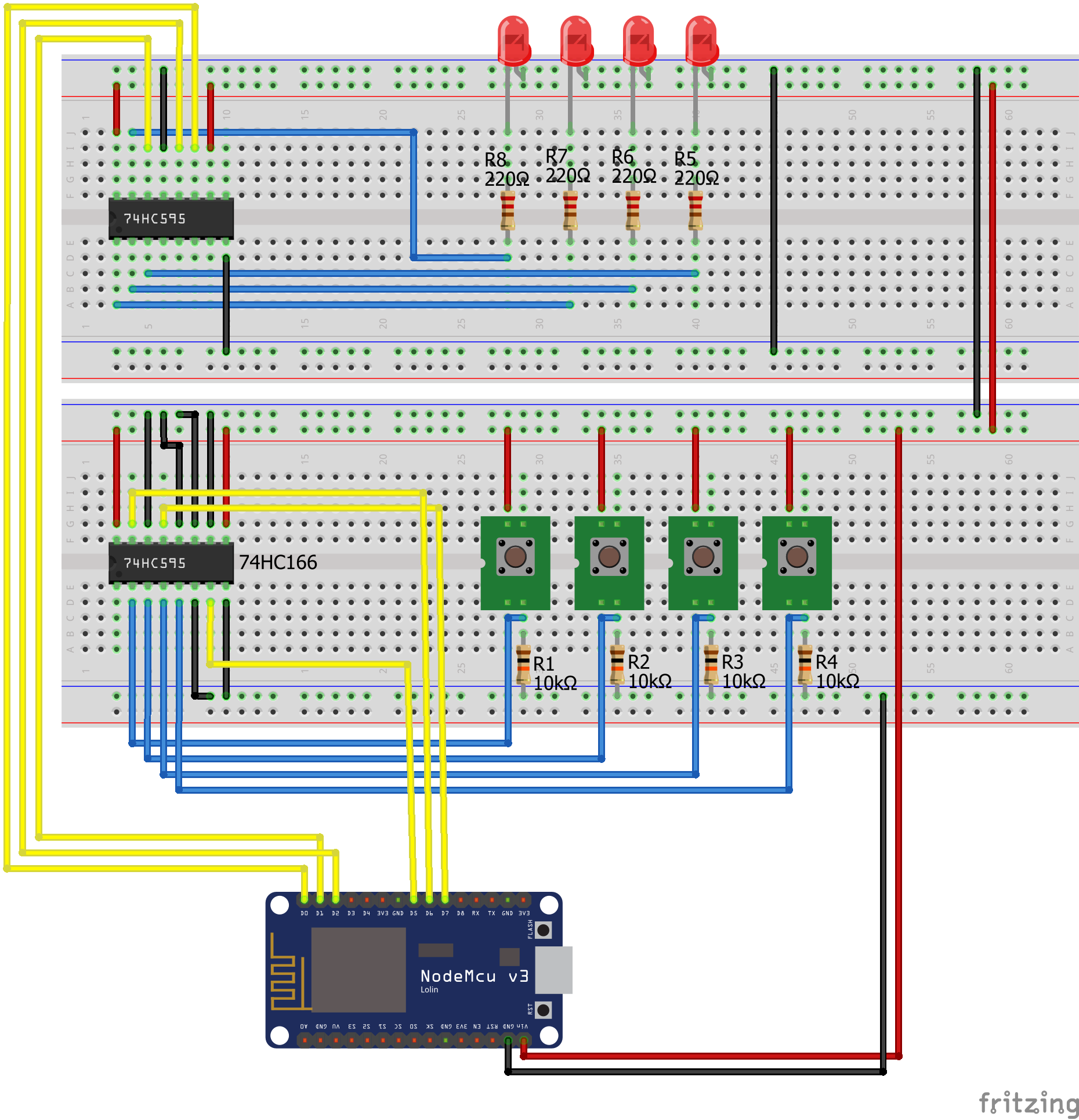
Shift Register SIPO PISO PullDown ESP8266 NodeMCU
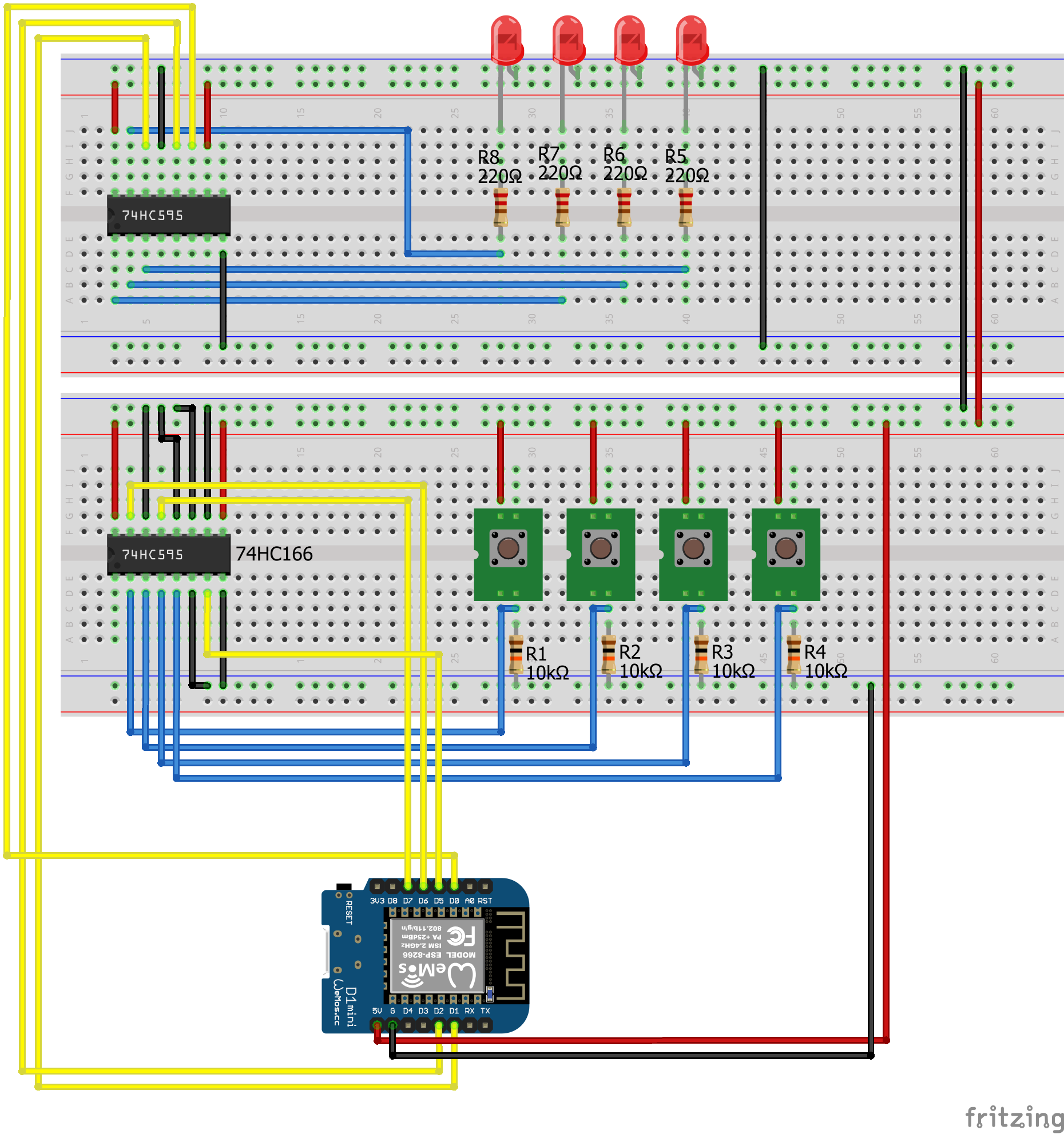
Shift Register SIPO PISO PullDown ESP8266 WeMos D1 Mini
Because I already explained most of the program code, I will concentrate only on the changes.
// for Arduino Microcontrollers
int latchPin_PISO = 3;
int clockPin_PISO = 4;
int dataPin_PISO = 2;
int latchPin_SIPO = 5;
int clockPin_SIPO = 7;
int dataPin_SIPO = 6;

// for ESP8266 Microcontrollers
//int latchPin_PISO = D6;
//int clockPin_PISO = D5;
//int dataPin_PISO = D7;
//int latchPin_SIPO = D2;
//int clockPin_SIPO = D0;
//int dataPin_SIPO = D1;

// for ESP32 Microcontrollers
//int latchPin_PISO = 18;
//int clockPin_PISO = 19;
//int dataPin_PISO = 5;
//int latchPin_SIPO = 21;
//int clockPin_SIPO = 23;
//int dataPin_SIPO = 22;

int i;
int j;
int value;
byte switchVar = 0;
byte leds = 0;


void setup() {
  pinMode(latchPin_PISO, OUTPUT);
  pinMode(dataPin_PISO, INPUT);
  pinMode(clockPin_PISO, OUTPUT);

  pinMode(latchPin_SIPO, OUTPUT);
  pinMode(dataPin_SIPO, OUTPUT);
  pinMode(clockPin_SIPO, OUTPUT);

  Serial.begin(9600);
}

void loop() {
  byte dataIn = 0;
  leds = 0;
  updateShiftRegister();

  digitalWrite(latchPin_PISO, 0);
  digitalWrite(clockPin_PISO, 0);
  digitalWrite(clockPin_PISO, 1);
  digitalWrite(latchPin_PISO, 1);

  for(j = 0; j < 8; j++) {
    value = digitalRead(dataPin_PISO);
    if (value) {
      dataIn = dataIn | (1 << j);
      }
      digitalWrite(clockPin_PISO, LOW);
      digitalWrite(clockPin_PISO, HIGH);
    }

    if (switchVar != dataIn)
    {
      switchVar = dataIn;
      Serial.print("dataIn DEC: ");
      Serial.print(dataIn, DEC);
      Serial.println();
      Serial.print("dataIn BIN: ");
      Serial.print(dataIn, BIN);
      Serial.println();

      if ((int) dataIn == 192) {
        i = 5;
      }
      else if ((int) dataIn == 128) {
        i = 6;
      }
      else if  ((int) dataIn == 64) {
        i = 7;
      }
      bitSet(leds, i);
      updateShiftRegister();

      for (int i = 7; i >= 0; i--)
    {
        bool b = bitRead(leds, i);
        Serial.print(b);
    }

    delay(1000);
    Serial.println(" ");
    }
}

void updateShiftRegister()
{
   digitalWrite(latchPin_SIPO, LOW);
   shiftOut(dataPin_SIPO, clockPin_SIPO, LSBFIRST, leds);
   digitalWrite(latchPin_SIPO, HIGH);
}
First of all we define the latch, clock and data pin for the PISO and SIPO shift register for the different microcontroller. The script is commented for Arduino microcontrollers. If you want to use an ESP8266 or ESP32 micocontroller, just uncomment the section for the PISO and SIPO pins and comment the Arduino lines.
After we define the PISO and SIPO pins, different variables are defined that we need during the script.
In the setup function the data pin of the PISO register is set as input and all other pins as output. The baud rate is set to 9600.
The loop function starts with the initialization of the dataIn variable to detect which buttons was pressed and set the variable to 0 in each iteration of the loop function because otherwise we do not detect a pressed button more than one time. Also after each cycle we set the leds variable back to 0 and update the shift register with the function we already know from the first example of this tutorial to turn off the LEDs again as well as enable the PISO shift register to read the states from the buttons.
You already know this part of the program from the PISO example. We check for each bit if the corresponding button is pressed and add all states via the bitwise OR operator. After we know which buttons are pressed we print the decimal and binary value to the serial monitor.
Now we combine the SIPO and the PISO example. After we know which button was pressed and the decimal value of this combination, we if else through all possibilities and match the button state with the variable i which lights up the corresponding LED via the bitSet function you also know from the SIPO example.
At the end of the script we print the bit array of the LEDs and wait for 1 second.
The last part of the script is the updateShiftRegister function that we use in the first example.
The following video shows me pressing different buttons to turn on the matching LEDs.
Conclusion
I hope you liked this tutorial and moreover I am happy if you learned how a shift register is working and what different kinds of shift registers are available. If you have any questions regarding this article, please use the comment section below to ask your questions.
If you are also interested how to increase the number of analog pins on your microcontroller which an analog multiplexer, then I can recommend this article.
You explanations are very well done.
Looking for an NTP time with the ESP and output to 595 onto four, seven segment LED display.
Keep up the great work.
Hi Za,
thanks for your comment. I will hold the quality high on my blog 🙂
Thanks for the write up. One critical thing on 595N.. As per datasheet, each output pin can only allow 7mA continuously at 1V, or, approximately 3mA at 3.3V (all supply voltage dependent). Therefore, 3-4 LEDs as indicated will not lid.
Hi Deniz,
where did you find this information in the datasheet? On page 6/22 that is linked, I only find the max output current for pins Qn (n: 0…7) is +- 35mA.
Hi where is ESP8266-01 module is not there in images above. My question is could it be used with shift register or not Thankyou
Hi, yes you could also use the ESP-01 as PISO or SIPO because you only need 3 digital I/O pins, see https://diyi0t.com/what-is-the-esp8266-pinout-for-different-boards/
Hi,
Wonderfully explained. I am working on a cable tester where a Flat Cable with 16 pins needs to be tested for continuity and shorts with Arduino Nano. Your use of SIPO and PISO together is exactly what is needed with SIPO (74HC595) sending HIGH to one end of each wire sequentially of the Flat Cable. The Arduino Nano reads the state of the other end of each wire of the Flat Cable with PISO (74HC166). However, my cable has 16 wires and hence I’ll need cascading 2x 595s and 2x 166s. Do you think this combination of 595 and 166 will suit this application? Can you help me with the code to synchronise the sending of sequential HIGH to one end and reading the state of the other end?